Condition:New
Type:Logic ICs
Model Number:ADF5355
Supply Voltage:5V
ADF5355 high frequency signal source color module
Module features:
1, ADF5355 module is a senior engineer to build, and fully refer to the official version of the design; PCB appearance beautiful, reasonable layout and design, with exquisite materials;
2, output frequency range: A+, A- output: 250M-6.8G, B output (A 2 octave output): 6.8G-13.6G; A output terminal output frequency resolution is 10Khz;
3, power supply mode: 5V power supply, can directly use USB power supply;
4, color display, touch screen operation, can realize frequency, sweep frequency (Special tip: it is recommended not to tear off the protective film on the screen, because the touch screen is a resistive screen, and scratches will cause the touch function to fail).
5, the module has save function, you can store the set parameters.
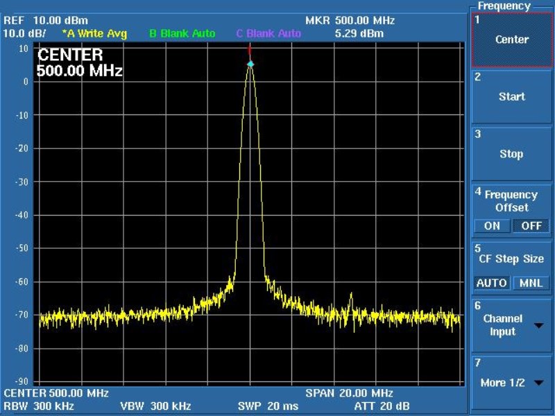
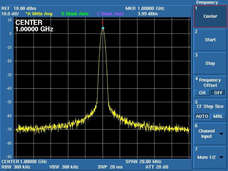
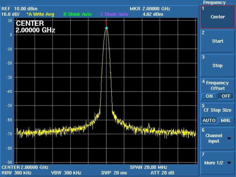
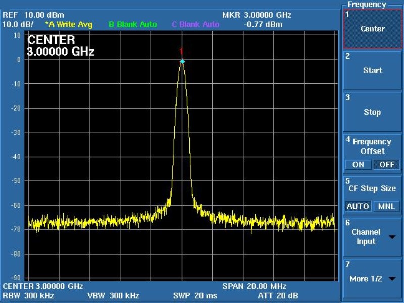
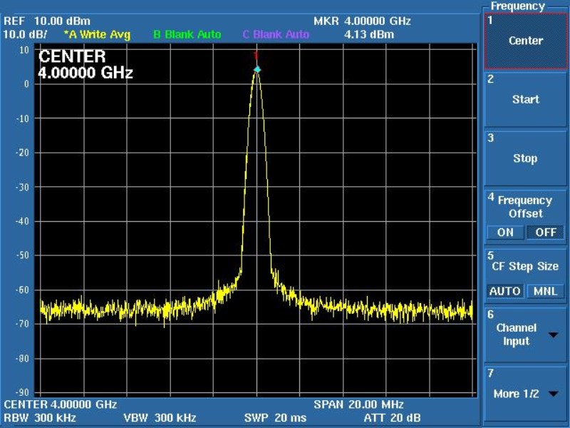
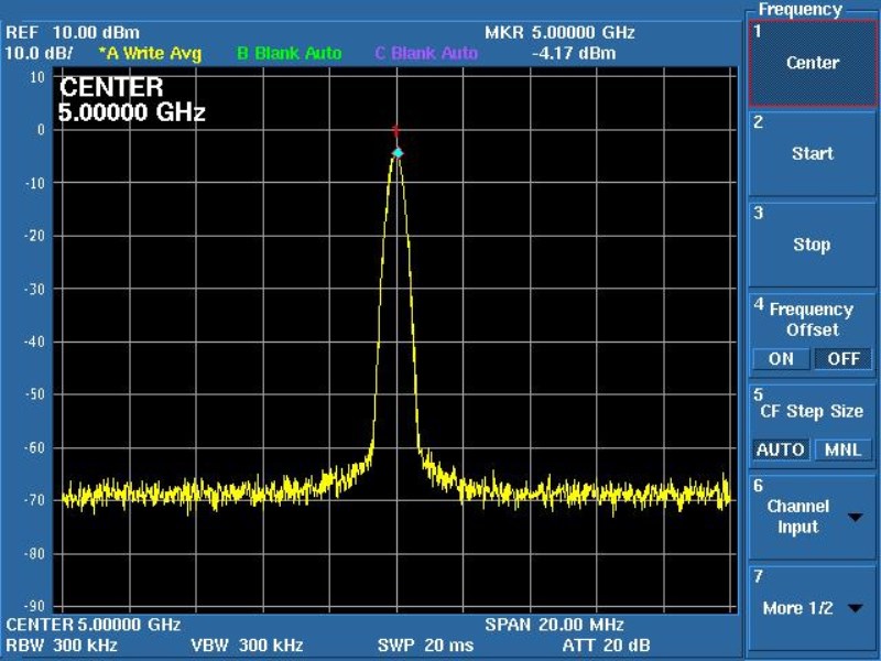
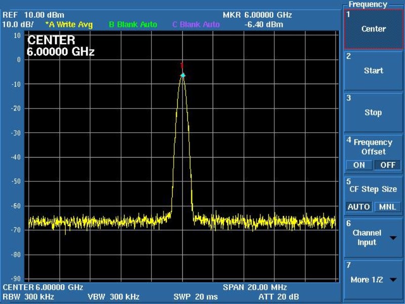
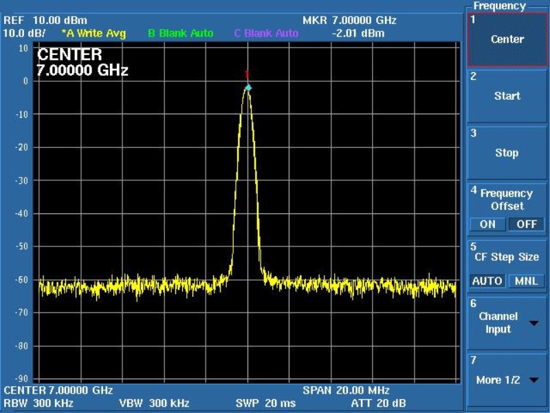
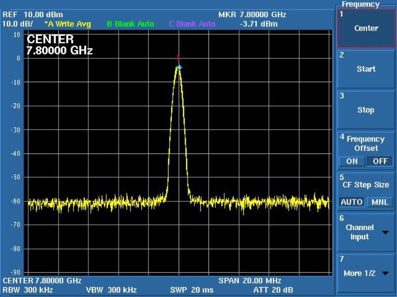
TwoModule measured waveform
500M
1Ghz
2Ghz
3Ghz
4Ghz
5Ghz
6Ghz
7Ghz
7.8G
Three. Application of module:
Wireless infrastructure (W-CDMA, TD-SCDMA, WiMAX, GSM, PCS, DCS, DECT)
Point to point to point to multipoint microwave links
Satellite /V-SAT
Test equipment / instrument
Clock generation
Four,Kit:
1, ADF5355 module one
2, USB line one
3. Provide: schematic diagram (PDF),No source program is providedProvides STM32 based ADF5355 underlying drivers, other information;
Five, chip introduction:
ADF5355 combines the external loop filter and the external reference frequency when it can be implemented with fractional N frequency division or integer N frequency division phase-locked loop (PLL) frequency synthesizers. The microwave broadband VCO design allows the implementation of an RF (RF) output at 6.8 GHz to 13.6 GHz operating frequency. A series of frequency dividers with other frequency outputs can achieve operating frequencies of 54 MHz to 6800 MHz.
The ADF5355 has an integrated VCO with a fundamental output frequency range of 3400 MHz to 6800 MHz. In addition, the VCO frequency can be divided into 1, 2, 4, 8, 16, 32 or 64 frequency division, so that the user can produce an output frequency of RF as low as 54 MHz. For applications requiring isolation, the RF output stage can mute. The mute function can be controlled either by pin or by software.
All on-chip registers are controlled by a simple three wire interface. The ADF5355 employs 3.15 V to 3.45 V analog and digital power supplies, and operates from 4.75 V to 5.25 V charge pump and VCO power supplies. In addition, ADF5355 has built-in hardware and software power saving mode.
RF output frequency range: 54 MHz to 13600 MHz
Fractional-N N frequency division synthesizer and integer N frequency division synthesizer
High resolution 38 bit modulus
Frequency discrimination phase detector (PFD) with operating frequency up to 125 MHz
The reference frequency is 600 MHz
In 40 ~ C and maintain the frequency range of C to +85 DEG
Low phase noise voltage controlled oscillator (VCO)
Programmable 1/2/4/8/16/32/64 frequency division output
?
Analog and digital power supply: 3.3 V
Charge pump and VCO power supply: 5 V (typ.)
Logical compatibility: 1.8 V
Programmable dual modulus prescaler: 4/5 or 8/9
Programmable output power
RF output mute function
Analog and digital lock detection
Remarks: the above is chip description, non module function description